After I first soldered the entire YCA2109 electronic dice, I connected power and pressed the button, but not one of the 7 LEDs lit up. More alarmingly, after continuing to power it for about 10 minutes, the two chips were clearly hot to the touch, though not yet hot enough to burn my hand.
The root cause finally confirmed was not in the solder joints or the button, but the two DIP chips sitting in the IC sockets were oriented incorrectly. After turning off the power, I flipped both the NE555P and CD4017BE 180 degrees, and the board lit up again; later, during full testing, the electronic dice was also able to stop randomly at different numbers.
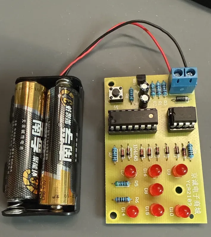
The YCA2109 circuit board with two AA batteries at first power-up; all 7 LEDs on the board were unlit.
First round of checks: confirm where power was actually being delivered
In the beginning I didn’t know whether the problem was in the power, the button, the soldering, or the chips, so I started with the easiest thing to measure: the power supply.
| Check item | Measured observation | What it indicated at the time |
|---|---|---|
| Each of the two batteries measured separately | About 1.5V each | The batteries did not appear to be completely dead |
| Battery holder measured after being disconnected from the circuit board | About 3V | The battery holder’s no-load output was normal |
| Battery holder terminals measured after being connected to the circuit board | 2.232V | The voltage dropped noticeably after connecting to the board |
| Whether the button was pressed or not | it stayed around 2.2V | The low voltage did not only appear when the button was pressed |
| I replaced the batteries with new ones | The result was still the same | The old batteries were not the only possible cause |
| I switched to three batteries | The board side still showed only about 2.4V | Adding more batteries did not bring the board voltage back to normal |
These readings did not directly tell me which component was installed incorrectly, but with the battery holder showing about 3V unloaded, dropping to about 2.2V after connecting to the board, and both chips heating up, it was clear I could not keep relying on pressing the button and hoping for luck. The problem seemed more likely to be in the circuit board or the assembly itself.
There is also a power supply boundary to clarify: TI’s NE555 datasheet lists the recommended operating voltage of the NE555P as 4.5V to 16V; the CD4017B datasheet gives a recommended range of 3V to 18V. Therefore, the nominal 3V from two 1.5V batteries was already below the recommended lower limit of the NE555P. But this cannot explain why the board still dropped to about 2.4V with three batteries, and it certainly cannot explain abnormal heating as a normal phenomenon.
Power off and inspect solder joints: photos can help observation, but they cannot replace measurement
After noticing the heat, I first disconnected the power, then turned the board over to inspect the back. In the photo, the power wires and terminal blocks did not appear to have obvious loose connections, and the shapes of some solder joints were not entirely uniform.
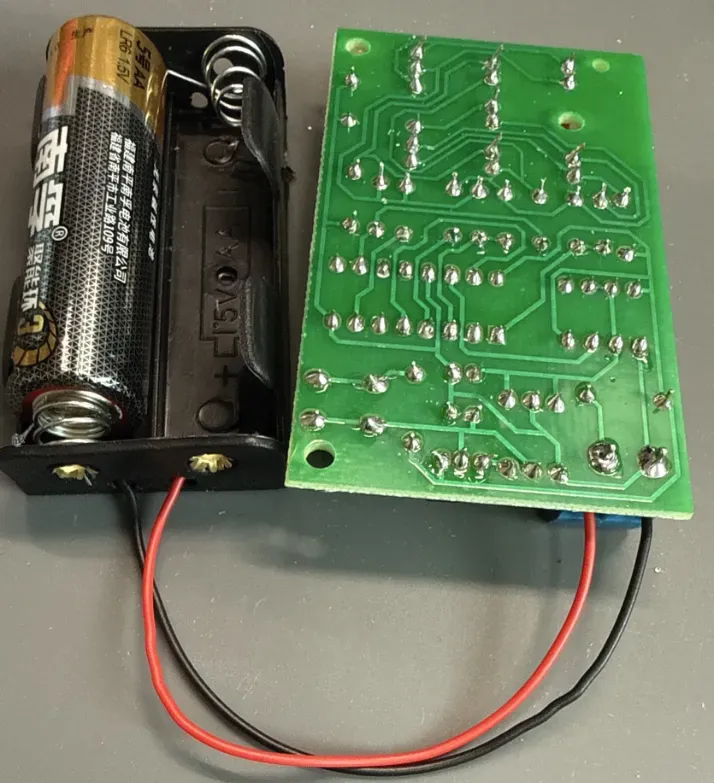
Back side of the board photographed after power-off, showing soldered through-hole component joints with trimmed leads.
However, based on this photo alone I cannot conclude that a particular joint is a cold solder joint or a short. The appearance of the solder joints can only help narrow the inspection scope; whether the electrical connections are normal still needs to be judged by continuity, voltage, and component orientation.
When checking with a multimeter, I first stepped into a mode trap
After powering off, I first measured continuity across the board’s power input terminals. When I swapped the red and black probes, the meter showed OL both times; when I touched the two probes directly together, the meter beeped. This showed that the probes and the continuity mode were working basically fine, but because the circuit input includes components such as diodes, seeing OL in both directions does not prove the whole board is fine.
Next, I measured the larger axial diode next to the blue terminal block. The first reading I got was ‘0.018F’ and ‘OL.’ Later, when I looked at the multimeter, I realized the knob was still on capacitance mode, and the screen was also showing nF.
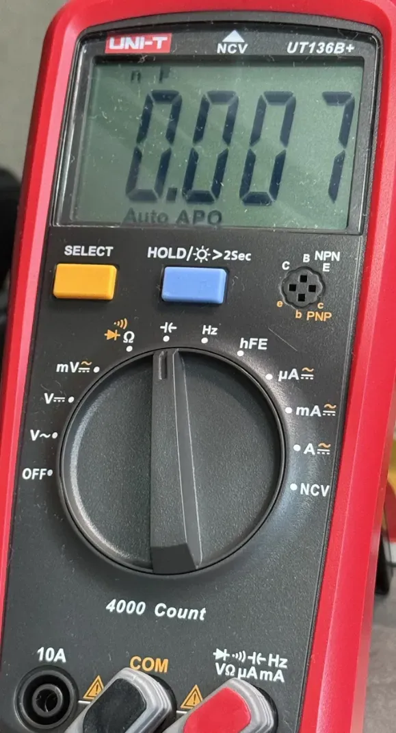
When I first checked the input diode, the UT136B+ was actually in capacitance measurement mode, so that reading could not serve as a conclusion about the diode’s condition.
After switching the dial to the true diode mode, I swapped the test leads and measured again: one direction read approximately 0.569V, and the other direction read OL.
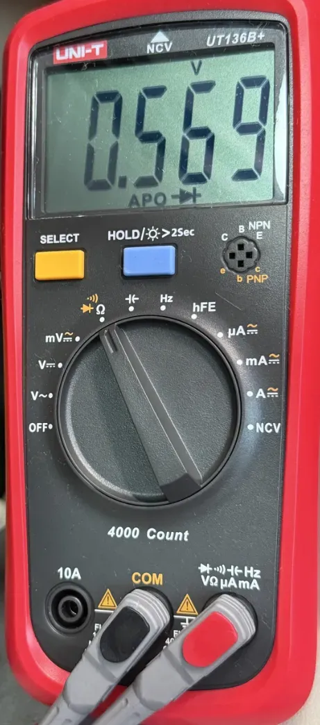
After switching to the diode mode, the multimeter screen showed the diode symbol and 0.569V; the other direction after swapping the leads read OL.
This result exhibited one-way conduction behavior, reducing the possibility of the input diode being shorted or open in both directions. But since it was measured directly on the circuit board without removing the diode for individual testing, I did not write it as a final determination of the component’s status.
The real turning point: I had been measuring electrical signals all along, but never confirmed the chip orientation
Up to this point in troubleshooting, the AI suggested I continue measuring the pins of the two chips. I didn’t actually execute that step, because the phrase “chip pins” first reminded me of something else: do the chips have an orientation? Did I really confirm that when I installed them?
I went back to the product page to check the product images and found that the orientation of the semicircular notch on both chips in the pictures was exactly opposite to mine. It turned out that even though I aligned the chip notch with the IC socket notch, I never continued to verify that the pin 1 reference of the IC socket, the PCB, and the chip actually corresponded.
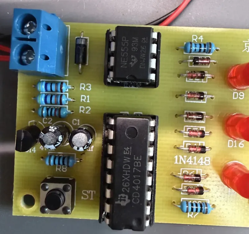
Close-up of the board surface in the fault state, showing the model numbers of the NE555P and CD4017BE chips, as well as the direction of their semicircular notches at that time.
DIP chips are not direction-independent like resistors. Taking the two chips on this board as an example, the top views in the TI datasheets show:
-
Pin 1 of the NE555P is GND, pin 8 is VCC, and the remaining pins are used for functions such as trigger, output, reset, threshold, and discharge.
-
In the CD4017B pinout corresponding to the CD4017BE, pin 16 is VDD, pin 8 is VSS, and the remaining pins include clock, reset, clock inhibit, and multiple decoded outputs.
When a chip is rotated 180 degrees, the circuit positions that each pin lands on will change. Pins that were originally meant for power, ground, or signals will connect to different traces, so the circuit may not work and may even heat up abnormally.
A more reliable installation method is not memorizing “notch to the left” or “notch toward the button.” Those absolute directions only make sense for one specific board orientation. What you really need to verify is the notch or dot on the chip package, the top-view pin numbering in the datasheet, and the pin 1 or orientation marker on the PCB.
After swapping the orientation of both chips, the electronic dice recovered
After powering off, I removed both the NE555P and CD4017BE chips, rotated each 180 degrees, and reinserted them into the IC sockets. After reapplying power, the LEDs finally lit up.
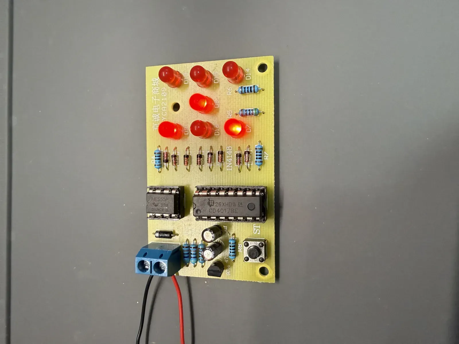
After swapping the orientation of both chips, the red LED on the YCA2109 circuit board successfully lit up.
After a short test, I powered off and waited about a minute; both chips were cold, and the obvious heating seen earlier did not recur. Later I fully tested the electronic dice: after a gentle press of the button, the lights run and stop at a random spot.
If I were to install it again, these are the checks I would do first
-
First confirm the power supply specifications and polarity; do not power up until confirmed.
-
Check each component that requires orientation one by one, including electrolytic capacitors, diodes, LEDs, transistors, and chips.
-
When installing a DIP chip, first find the notch or dot, then confirm pin 1 according to the datasheet and PCB markings — don’t rely only on the IC socket.
-
After applying power for the first time, first observe lights, sounds, smell, and temperature; if abnormal heat appears, cut power immediately.
-
Before using a multimeter, check the knob position, screen symbols, and units, so you don’t continue reasoning with a reading from the wrong range.
-
When troubleshooting, try to change only one condition at a time, and record the results before and after the change. That way, after restoring, it’s easier to pinpoint the real cause.
This time my biggest lesson is simple: every pin on a chip has its own purpose. When installing, you must first distinguish the orientation — you can’t just pick any direction and connect it while you’re still confused.
For complete beginners, not knowing every component isn’t scary. The real danger is repeatedly applying power without confirming orientation and supply. Stopping first, then narrowing things down step by step based on evidence, is more reliable than constantly swapping batteries, pressing buttons, or guessing answers.